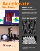
NanoFraction has unveiled the PHASE platform, powered by its groundbreaking Digital Holographic Optical Moiré (DHOM) technology, to address the semiconductor industry's biggest challenges: dark silicon and the limitations of traditional SEM. Combining multi-scale nanoscale discovery, AI-driven super-resolution, and advanced collaboration tools, PHASE empowers researchers and manufacturers to accelerate innovation, improve defect detection, and optimize semiconductor production.
SAN DIEGO, Nov. 21, 2024 /PRNewswire-PRWeb/ -- For decades, the semiconductor industry has faced two critical challenges: the hidden limitations of dark silicon and the bottlenecks of Scanning Electron Microscopy (SEM) in defect detection and quality control. NanoFraction, , a leader in nanoscale innovation, proudly unveils the PHASE platform, powered by the revolutionary Digital Holographic Optical Moiré (DHOM) technology, to overcome these challenges and drive the industry forward.
Breaking the Double Barrier: Dark Silicon and SEM
Dark silicon—where portions of chips remain unpowered due to power and thermal constraints—has long hindered the industry's ability to optimize chip architectures. Compounding this issue, traditional SEM, while invaluable for material characterization, often struggles to meet the speed and scalability demands of modern semiconductor production. Together, these barriers slow progress and keep semiconductor innovation in the shadows.
NanoFraction's PHASE (Physics-based Holography and AI Super-resolution Engine) platform redefines the possibilities of nanoscale discovery and defect detection, offering faster, more scalable solutions for today's challenges.
Introducing DHOM: The Core of the PHASE Platform
At the heart of PHASE lies Digital Holographic Optical Moiré (DHOM), an advanced technology that combines an ensemble of robotic nanoscopes and a neural compute grid to deliver multi-scale digital twins of materials like diamond and silicon carbide. By scanning at millimeter, micron, and nanometer levels, DHOM achieves a world-first resolution of 1 nanometer.
Building on this robust foundation, PHASE integrates:
- AI Super-Resolution Stack: Combines physics-based optical super-resolution with AI-driven techniques for unparalleled accuracy and scalability.
- Collaborative SaaS Framework: A secure, scalable software platform enabling seamless remote collaboration, data sharing, and integration with modern AI pipelines like Jupyter notebooks.
"Our DHOM technology represents a paradigm shift in nanoscale discovery," said Eduardo Sciammarella, CEO of NanoFraction. "From R&D to production, we're enabling manufacturers to streamline workflows, reduce costs, and unlock the full potential of advanced materials."
Driving Semiconductor Innovation
Advanced Capabilities for Diamond and Silicon Carbide
NanoFraction's platform can detect over six species of defects in diamond wafers, providing critical insights into their mechanical, electronic, and thermal properties. These insights accelerate the discovery pipelines in R&D and ensure a seamless transition to high-volume production—a feat unattainable with traditional SEM.
As the industry transitions from standard silicon wafers to hybrid architectures, such as silicon carbide and diamond, these advanced materials are critical for improving thermal conductivity, power efficiency, and durability in AI chips and high-performance computing systems.
Addressing Overheating and Yield Optimization in AI Chips
Heat generation in chips, often a byproduct of data erasure, underscores the importance of defect-free material architectures. NanoFraction's defect detection technology ensures that manufacturers can fine-tune production processes, reduce defects, and enhance thermal management, resulting in higher-quality chips with greater energy efficiency and reliability.
Built for Researchers, Manufacturers, and Collaboration
The PHASE platform isn't just faster—it's smarter and more connected. It integrates effortlessly with modern AI pipelines, such as Jupyter notebooks, and supports remote collaboration with robust data security and an intuitive UX. PHASE's hardware stack includes:
- Nvidia Jetson ORIN platforms for compute performance.
- Dover Motion components for nanoscale precision.
- Optical systems from Hirox, the pioneer of digital microscopy.
This powerful combination ensures reliability and scalability from R&D discovery through high-volume production, future-proofing the semiconductor industry.
Call to Action
Are SEM and dark silicon slowing you down? Explore how NanoFraction's PHASE platform can revolutionize your defect detection and material characterization workflows. Visit or contact us at [email protected] to learn more or schedule a demonstration.
About NanoFraction
NanoFraction is at the forefront of nanoscale discovery and semiconductor defect detection. By combining DHOM technology with the collaborative PHASE platform, NanoFraction empowers researchers and manufacturers to overcome the challenges of dark silicon and achieve breakthroughs in material characterization and production quality.
Media Contact
Jenny Ventura, NanoFraction, 1 (949) 346-1585, [email protected],
SOURCE NanoFraction


Share this article